

In my fifteen years doing electronics repair, I’ve seen the same pattern repeat. Equipment shows clear symptoms—performance degradation, unexpected heat, battery drain—but traditional diagnostic tools come up empty. Multimeters show normal readings. Oscilloscopes display clean signals. Yet something is wrong.
The problem is that current leakage often occurs at levels too small for conventional tools to detect. We’re talking about faults drawing just a few milliamps, creating temperature rises of less than one degree Celsius. According to recent data from the IPC (Association Connecting Electronics Industries), over 40% of PCB failures originate from these micro-level electrical anomalies.
I watched a consumer electronics manufacturer in Los Angeles face a massive recall because they didn’t catch these subtle leaks during quality control. The cost exceeded half a million dollars—all from issues that would have been immediately visible with proper thermal imaging.
This is where thermal imaging technology transforms the game. Heat doesn’t lie. Any electrical abnormality generates thermal signatures, and modern phone thermal cameras can detect temperature differences as small as 0.05°C.
The Day I Stopped Doubting Phone Thermal Cameras
Three years ago, I was skeptical about phone-based thermal imaging devices. Professional handheld units cost thousands of dollars. How could a smartphone accessory possibly deliver the same precision?
My perspective changed completely in a New York phone repair shop. I watched a technician diagnose an iPhone battery management chip failure in under five minutes using a phone thermal camera. The process was smooth, accurate, and completely professional—no different from using a dedicated handheld unit.
But here’s what I learned: not every phone thermal camera can handle electronics work. Many are designed for building inspections, HVAC diagnostics, or finding drafts in your house. Those applications don’t require the precision needed for PCB-level work.
The National Institute of Standards and Technology has published extensive research on thermal imaging accuracy for electrical systems. Their findings confirm that consumer-grade thermal technology has advanced dramatically in recent years—but only specific implementations work for circuit board diagnostics.
Three Technical Specifications That Actually Matter
When I consulted for an automotive electronics company in Texas, they asked me to help them choose thermal imaging equipment. I created a checklist based on real-world testing with over thirty different models. These are the three specifications that determine whether a phone thermal camera can actually diagnose PCB issues.
Macro Focus: Your Gateway to PCB Clarity
Most thermal cameras can’t focus closer than about twelve inches. That’s fine for checking your home’s insulation or finding hot spots in an electrical panel. It’s completely useless for PCB work.
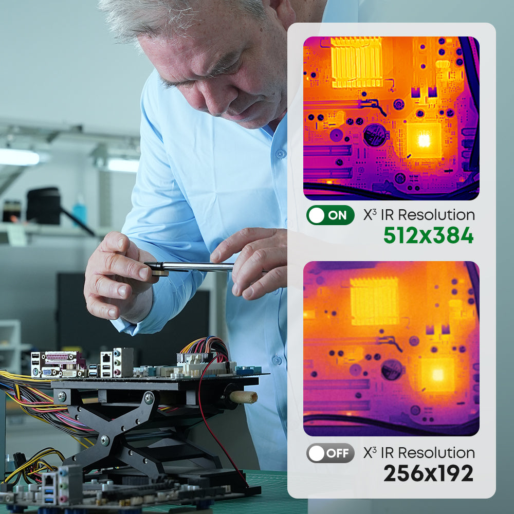
Modern circuit boards pack components into incredibly dense layouts. Individual resistors, capacitors, and integrated circuits sit just millimeters apart. At twelve inches, your thermal image becomes a blurry mess of color blocks—you can’t tell which specific component is generating heat.
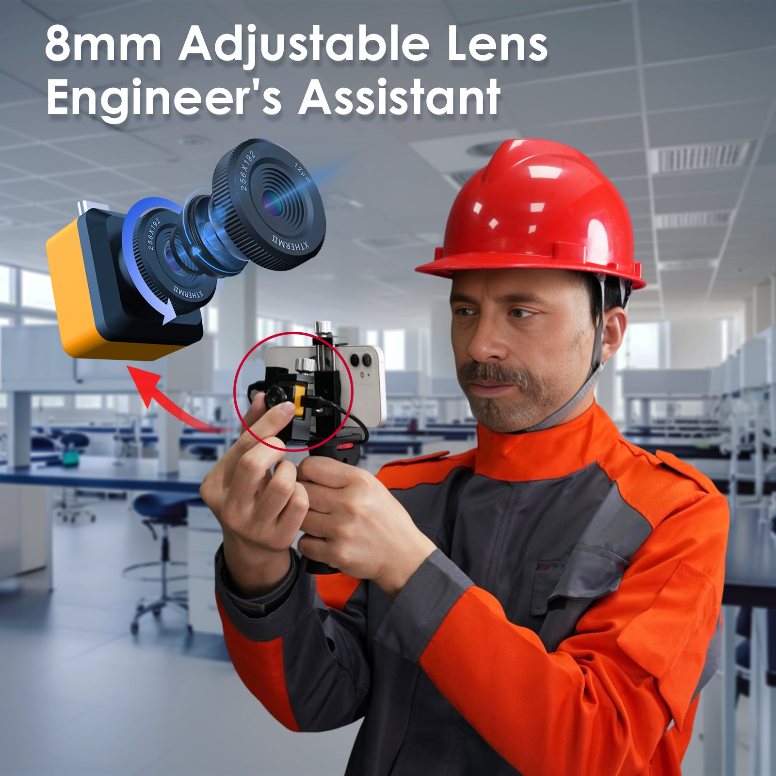
The phone thermal cameras that work for electronics repair typically feature 8mm manual-focus macro lenses. This allows you to get within a couple of centimeters of the board while maintaining sharp focus. At this distance, you can see thermal patterns on individual chip pins and trace routes.
Last month, I used macro thermal imaging to diagnose a laptop motherboard for a customer in Seattle. The fault was in a single decoupling capacitor next to the CPU. Standard focus thermal cameras would have shown the entire area around the CPU as hot. With macro focus, I could pinpoint the exact component.
Thermal Sensitivity: Seeing the Invisible
This specification determines whether you can detect subtle temperature variations. It’s measured as NETD (Noise Equivalent Temperature Difference)—the smaller the number, the more sensitive the camera.
Here’s a real-world example. Last year, I diagnosed a smart watch prototype for a San Francisco startup. They had an intermittent fault that only appeared after twenty minutes of operation. The temperature rise on the faulty component was less than 0.3°C above ambient. A thermal camera with poor sensitivity would never show this.
According to research from IEEE (Institute of Electrical and Electronics Engineers), detecting current leakage in modern low-power circuits requires thermal sensitivity of at least 0.1°C or better. Higher-end phone thermal cameras now achieve this specification.
Resolution: The Difference Between Guessing and Knowing
Thermal resolution determines how many individual temperature measurement points your image contains. This is separate from the display resolution you see on your phone screen.
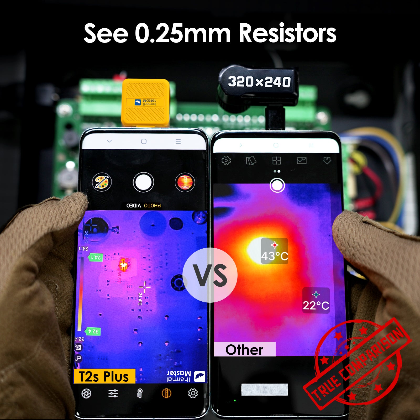
A typical entry-level thermal camera might have 80×60 pixel resolution. That’s 4,800 measurement points spread across your entire field of view. On a densely populated PCB, multiple components fall within each pixel, making it impossible to isolate the heat source.
Professional-grade phone thermal cameras now offer native resolutions of 256×192 pixels or higher. Some use digital enhancement algorithms to achieve even higher effective resolution. I tested this difference side-by-side at a Boston electronics repair conference last year. The improvement in diagnostic capability was dramatic.
How I Actually Use Thermal Imaging for PCB Diagnostics
After hundreds of PCB repairs using thermal imaging, I’ve developed a systematic approach that consistently finds faults quickly. Here’s my actual process.
Step One: Environmental Setup
I work in a temperature-controlled space away from direct sunlight and air vents. External heat sources create false thermal patterns that can mislead your diagnosis. I also ensure the PCB is powered and operating under the same conditions where the fault occurs—sometimes problems only appear under load.
Step Two: Camera Configuration
This step is where most people make mistakes. PCB substrate material has an emissivity around 0.95, which you need to set in your thermal imaging app. I manually adjust the macro focus until I see sharp detail on the components I’m inspecting. Many phone thermal cameras also offer image enhancement modes—I always enable these for maximum clarity.
Step Three: Systematic Scanning
I don’t just point the camera randomly. I scan methodically, starting with power delivery circuits, then moving to signal processing components. I pay special attention to components that appear in multiples—like RAM chips or capacitor banks. If one chip in a row is noticeably warmer than its neighbors, that’s usually your culprit.
Last month in Chicago, I diagnosed a server motherboard with this technique. Eight identical voltage regulators lined up in a row. Seven showed temperatures around 45°C under load. One peaked at 67°C. That anomaly led me directly to a manufacturing defect in that specific regulator.
Step Four: Documentation
Modern thermal imaging apps let you capture still images and record video of your findings. I document everything before starting any repair. This serves multiple purposes: proving the fault to customers, planning the repair strategy, and verifying the fix afterward.
The Occupational Safety and Health Administration requires documented thermal inspections for many commercial electrical systems. While consumer electronics aren’t under the same regulations, maintaining professional documentation standards builds customer confidence.
Step Five: Comparative Analysis

One technique I use constantly: comparing thermal patterns between identical components or between known-good and suspect boards. This relative comparison often reveals subtle anomalies that absolute temperature measurements might miss.
What Makes a Phone Thermal Camera Actually Worth Buying
After testing dozens of models over the past five years, I’ve learned which features separate useful tools from expensive paperweights. When repair professionals ask me for recommendations, here’s what I tell them.
First, ignore marketing hype about “military-grade” or “professional-level” specifications. Focus on three verified metrics: minimum focus distance (should be 8mm or less for PCB work), thermal sensitivity (NETD of 0.1°C or better), and native sensor resolution (256×192 minimum).
Second, consider battery life and workflow integration. Some phone thermal cameras draw significant power from your device. Others include their own batteries. I prefer models that can run for several hours without draining my phone—essential for longer diagnostic sessions.
Third, evaluate the accompanying software. The best hardware in the world is useless if the app crashes constantly or lacks basic features like adjustable emissivity settings, temperature spot measurements, and report generation.
The Thermal Master P3 checks all these boxes. I’ve used it extensively for the past eighteen months, and it’s become my primary diagnostic tool. The 8mm macro lens delivers genuinely sharp PCB imaging. The enhanced resolution mode provides detail I previously only got from dedicated handheld units costing five times as much.
Frequently Asked Questions
Can thermal cameras see through components?
No, thermal cameras detect infrared radiation from surfaces. They can’t see through objects. However, heat conducts through materials, so a hot component underneath something may warm the surface above it, creating a detectable thermal signature.
How long does it take to learn thermal diagnostics?
Basic interpretation—identifying hot spots and temperature anomalies—you can learn in an afternoon. Professional-level diagnosis, where you understand the implications of specific thermal patterns and can trace root causes, develops over months of practice with real-world failures.
Are phone thermal cameras as accurate as handheld units?
Modern high-quality phone thermal cameras match or exceed the accuracy of mid-range handheld units for temperature measurement. Where handhelds still have advantages is battery life, ruggedness, and sometimes in optical quality. But for pure diagnostic capability in controlled environments, the gap has largely closed.
What maintenance do thermal cameras need?
Very little. Keep the lens clean—thermal sensors are particularly sensitive to dirt and fingerprints. Store the device in moderate temperatures. Some models with built-in batteries need periodic charging even when not in use. That’s about it.
Can I use thermal imaging on powered boards safely?
Yes, this is standard practice. Thermal imaging is non-contact and doesn’t interact with the circuit. However, you still need to follow normal electrical safety practices when working around powered electronics. The thermal camera itself poses no additional risk.